

Presentation du DevKit Achilles SoC Arria ® 10
Le DevKit Achilles SoC Arria® 10 est basé sur le FPGA Intel® Arria® 10 SoC. Il comprend le module Achilles Arria® 10 SoC, une starter board, ainsi que tous les schémas et designs de référence utiles pour commencer à travailler avec la carte.
Avec son ARM double-coeur Cortex-A9 MPCore et jusqu’à 660 KLEs dans le FPGA d’éléments logiques à faible consommation, le PFGA Arria® 10 SoC combine la flexibilité et la facilité de programmation d’un CPU avec la configurabilité et la puissance de traitement parallèle d’un FPGA.
Grâce à son SoC (system-on-chip) (un circuit intégré à l’intérieur du FPGA, le plus souvent un processeur CPU – central processing unit), le FPGA peut mieux contrôler la carte.
Sa petite taille et son FPGA puissant le rendent parfaitement adapté aux marchés de l’embarqué et de l’industrie.
Les marchés cibles incluent l’industrie automobile, la diffusion vidéo, la vision intelligente par ordinateur, l’industrie, le militaire, les tests & mesures, et le medical.
Le module Achilles Arria 10 SoC peut aussi être acheté seul. Nous vous proposons aussi en option la carte porteuse PCIe, compatible avec tous nos modules Arria® 10 SoC de reflex ces. Nous pouvons sinon vous concevoir une carte porteuse sur-mesure.
La famille de FPGA Intel® SoC Arria® 10 intègre un ARM Cortex-A9 MPCore double-coeur, ainsi que des microcontrolleurs à programmation logique haute-performances, avec transceivers haute-vitesse intégrés.
Le DevKit Achilles de reflex ces offre de nombreuses interfaces selon vos besoins et exigences.
Ce Kit de développement a de nombreux avantages. Il peut être utilisé comme une carte d'évaluation pour commencer à tester votre design, pour réduire votre délai de mise sur le marché. Il peut aussi être utilisé comme une carte de développement, pour faire du prototypage.
Toutes les fiches produits dont vous pourriez avoir besoin seront fournis dans un board support package (BSP). Notre équipe technique est aussi disponible en ligne sur https://support.reflexces.com/
Le FPGA Arria® 10 SoC est un semiconducteur qui permet d'économiser de l'espace sur la carte, avec une densité doublée par rapport à la génération précédente. Cependant, ses besoins énergétiques sont inférieures, et donc sa consommation d'énergie l'est aussi.
le Devkit Achilles est conçu pour une forte productivité, et est parfaitement adapté aux marchés de l'embarqué et de l'industrie.
Notre DevKit Arria® 10 SoC est donc spécialement conçu pour les besoins du client. Notre équipe commerciale est disponible pour vous recommander la meilleure solution en fonction de vos besoins, n'hésitez pas à les contacter sur sales@reflexces.com.
A découvrir sur rocketboards :
Block diagram du DevKit Arria ® 10 SoC:
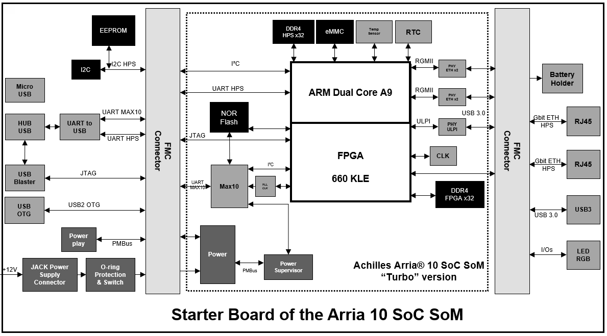
Processor
FPGA
FPGA & Soft programming
Control & Ios : Arria® 10 SoC SoM
Main interfaces 1.8V FMC VITA 57.1 compliant* :
System-on-Module usage:
Carrier board usage with 2 interfaces:
24 Transceivers (up to 11.3Gbps):
LVDS and LVCMOS
Memory
Communications & interfaces : Arria® 10 SoC SoM + starter board Arria® 10 SoC SoM
Power
Form factor : Arria® 10 SoC SoM
Form factor : Arria® 10 SoC SoM + starter board Arria® 10 SoC SoM
Standards and compliance
In addition of the Achilles DevKit, you can order the PCIe Carrier Board
* There are four FMC connectors , but the two mirror connectors (Top and Botom on each side) share the same signals, the use of these two connector sis exclusive, one of the two connectors can be used at a time.
Arria® 10 SoC disruptive System-on-Module by REFLEX CES :
Achilles Workshop by REFLEX CES :
Setting up your REFLEX CES Achilles Development Kit :
Exploration of REFLEX CES' Graphical User Interface (GUI) for the Achilles Development Kit :
Object detection demo using FPGA DNN IP :
Livrables
Informations de commande
Numéro ECCN : 4A994i
CECC (commodity Export Classification Certificate) : Télécharger certificat
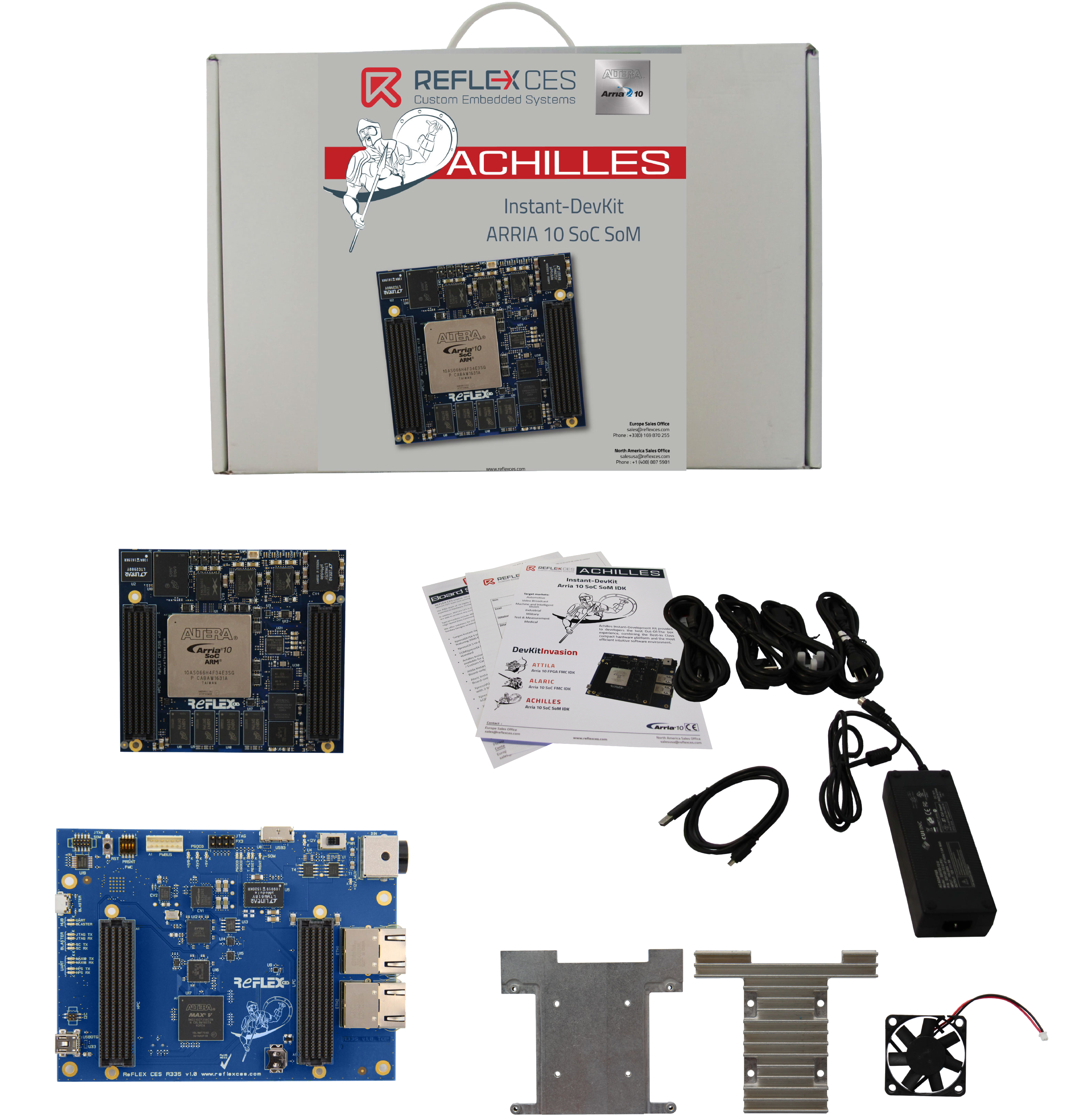
The Achilles Instant-Development Kit, based on the A10 SoC SoM Turbo version, provides to developers the best Out-Of-The-Box experience, with all the parts that a customer can require to start the System-On-Module.
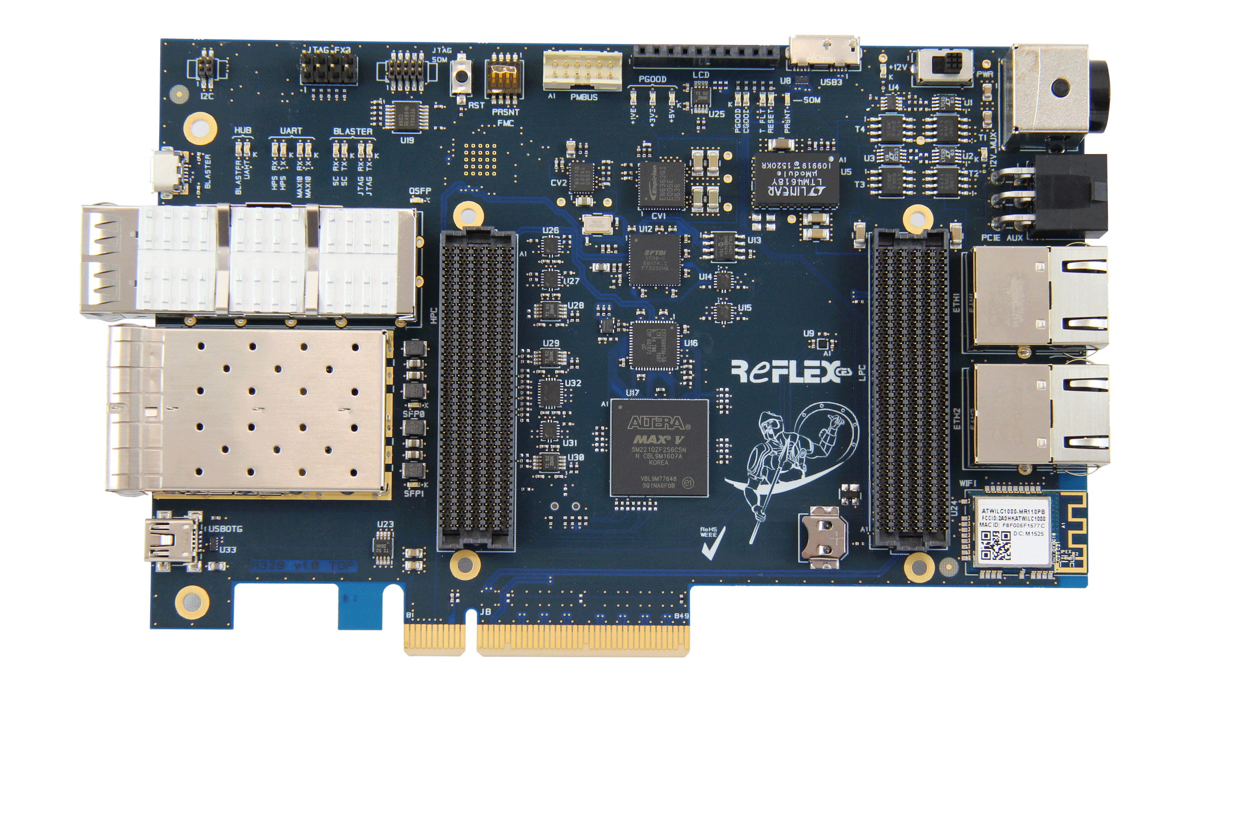
The Achilles DevKit is delivered with a starter board that provides all the interfaces to communicate with the FPGA and the HPS
-> For more details about the Achilles SoM module main features and to get documentation, please email sales@reflexces.com or go on www.reflexces.com/contact
The Achilles Instant-Development Kit includes the following elements:
When you purchase an Achilles Development Kit, it will also include the Starter board. The starter board includes:
The Arria® 10 SoC SoM offers several versions that depends on the FPGA performances needs and the use of the board.
Lite version: provides the industry’s lowest system cost and power, along with performance levels that makes the device family ideal for differentiating your high-volume applications.
Turbo version: provides high processing capabilities with the 600KLEs and DDR4 high performances levels that makes the device family ideal for complex applications. The dual FMC capabilities allows to interconnect this module very easily with the complete system.
Industrial version: provides industrial temperature product that allows you to use FPGAs and CPLDs, memories and complete design in high-temperature environments, such as automotive telematics, infotainment, and driver assistance systems, as well as temperature-sensitive military and industrial applications.
-> For more details about the module versions and to get documentation, please email sales@reflexces.com or go on www.reflexces.com/contact
The dual FMC capability is the latest idea of REFLEX CES and it takes shape through Achilles : The module can be plugged on a customer carrier board with the two FMC bottom connectors, and offers front panel IO possibilities with a mix of FMC modules plugged on the two FMC Top connectors
The Achilles System-On-Module can be used as FPGA Mezzanine Card & carrier board at the same time!
Do not forget that there are four FMC connectors, but the two mirror connectors (Top and Bottom on each side) share the same signals, the use of these two connectors is exclusive, one of the two connectors can be used one at a time.
Typically, the panel IO functionality was fixed in form factor cards, or it was configured with a fixed front panel IO module. Changing the front panel IO functionality means replacing the complete system. The FMC allows us to create dedicated processing bridge for a wide range of Input / Output data, video , audio, networking and many others signals processing without replacing the all system.
The dual FMC capabilities provides a flexible solution allowing multi configurable I/O front-end for FPGAs
A FMC SoM can provide a flexible solution for custom carrier boards and avoids a long and complicated time to design the digital heart of the system.
A SoM is a highly integrated System-on-Chip module that can be considered as computer-on-module technology coupled with FPGA flexibility for more complex projects.
If you design a baseboard on which the Achilles SoC module will be installed, you need to provide SEAF Female connectors (the module is equipped with SEAM on its bottom side)
To obtain a total stack Height of 10 mm between the carrier board and the module, you must use the following reference: SAMTEC P/N: ASP-134486-01 (SEAF-40-06.5-10-A)
To obtain a total stack Height of 7 mm between the carrier board and the module, you must use the following reference: SAMTEC P/N: SEAF-40-05.0-10-A
-> If you want to have a different stack height, you must use the family SAMTEC SEARAY SEAM/SEAF connector; please refer and ask to the REFLEX CES support to know all the possible stack-height
If you design a Mezzanine board which is installed on Top of the Achilles SoC module, you need to provide SEAM Male connectors (the module is equipped with SEAF on its top side)
To obtain a total stack Height of 10 mm between the carrier board and the module, you must use the following reference: SAMTEC P/N: ASP-134488-01 (SEAM-40-06.5-10-A)
-> An Excel sheet with legends that describes what kind of signals are connected to the FPGA: LVDS, LVCMOS to standard Bank IOs FPGA, Transceivers to the XCVR bank FPGA, HPS is available upon request: Please contact the sales team to obtain more details on this topic at sales@reflexces.com or go on www.reflexces.com/contact
-> For more details about the FMC pinouts assignment and to get documentation, please email sales@reflexces.com or go on www.reflexces.com/contact
-> An Excel sheet with legends that describes what kind of signals are connected to the FPGA: LVDS, LVCMOS to standard Bank IOs FPGA, Transceivers to the XCVR bank FPGA, HPS is available upon request : Please contact the sales team to obtain more details on this topic at sales@reflexces.com or go on www.reflexces.com/contact
-> For more details about the FMC pinouts assignment and to get documentation, please email sales@reflexces.com or go on www.reflexces.com/contact
-> An Excel sheet with legends that describe what kind of signals is connected to the FPGA: LVDS, LVCMOS to standard Bank IOs FPGA, Transceivers to the XCVR bank FPGA, HPS is available upon request. Please contact the sales team to obtain more details on this topic.
-> For more details about the FMC pinouts assignment and to get documentation, please email sales@reflexces.com or go on www.reflexces.com/contact
You need to use the SEARAY™ High-Speed High-Density Array Cable Assembly from Samtec. Please refer to the SAMTEC web page HDR Cable Assembly Options for FMC to know all the interconnect possibilities.
This PCIe Carrier Board is an optional extra product for clients looking for a PCIe format board.
REFLEX CES Arria® 10 SoC module can be plugged on this PCIe Carrier Board. The PCIe carrier board then provides access to all of the features of the System-On-Module:
It also provides access to further functions, including:
The PCIe carrier board is delivered with schematics and VHDL test designs
-> For more details about the Achilles Instant DevKit and to get documentation, please email sales@reflexces.com or go on www.reflexces.com/contact
You will have two independent memory banks with four chips with density 8Gb or 16Gb each bank : each memory bank of the Arria® 10 SoC SoM address a 32 bits data bus width by using two chip x16bits, with a clock rate at 1200MHz or 2666MHz (according to the module version)
A test design that validates the DDR4 memory connected to the FPGA is available, it uses the Intel example design generated with the DDR4 controller IP.
The final user can use the memory bank connected physically to the HPS without using the HPS to add this memory interface to the FPGA. The DDR4 interface of the HPS uses the Bank IO, shared with the FPGA, and that can be used by the FPGA only. If the HPS is alive, the DDR4 is normally used to execute the Operating system pattern and cannot be used as additional memory interface to the FPGA.
Already mounted, the thermal solution is composed of two parts: Heat spreader and Heat sink, that offers air-cooled and conduction-cooled solutions depending of the customer environment.
If you want to use the SoM A10 in standalone application, on a desk or ambient environment without mechanical constraint, you can leave the FAN top of the set and ensure a good cooling solution.
If you want to integrate the SoM A10 into an enclosure, a server, or a custom rack, you need to evaluate the operating range temperature with requirements in terms of airflow. The heatsink can be upgraded by customization, to offer better airflow evacuation.
For highly constrained industrial environments, please refer to industrial version of the SoM, called “industrial”
This document provides information for designing a custom Carrier Board for the Arria® 10 SoC SoM Module. It includes reference schematics for the external circuitry, required to implement the different interfaces available on the module.
This design guide is intended for electronics engineers designing a carrier board for the Arria® 10 SoC SoM. In most cases, the examples come from designs that have been built and tested.
The CDG gives a list of suggestions for designing with high-speed differential signals and single ended signals:
The PHY component is connected to the Core Fabric of the Arria® 10 SX, the GPIF II interface is fixed at 8 bits on the PHY. This enables interface frequencies up to 100 MHz so a maximum work data rate of 800 Mb/s data rates after encoding, corresponding to High-Speed mode.
In case of redesign or creation of a similar interface by using the FMC interfaces, we advise to use the complete data bus of the FX3 by using the 32 bits to provide SuperSpeed solution with a symbol rate up to 5 Gbit/s for an effective data rate at 4 Gbit/s (500 MB/s).
When using the module alone without using our Starter board, you can supply the SoM A10 with an input voltage in the range of +5.5V-17V.
The components at the top in the power supply tree can absorb an input up to +17V. But, in this case, you will not be able to connect FMC modules to the TOP connectors of the module because VITA57.1 imposes a maximum of + 12V +/- 5%. In addition, to offer the input voltage for the internal power tree, we connect the + Vin directly to the pins of the FMC connectors. So be careful when designing your own power supply input and limitation.
When using a starter board or PCIe carrier board designed by REFLEX CES, you will see that we have a protective, surge and reverse mounting. You will be able to supply an input voltage in the range of + 9.5V-13.45V
Concerning the Arria® 10 SX SoM, we use power supply unit with a CUI INC AC adapter:
P/N: SDI120-12-U
Input: 100-240V ≈ 47-63Hz 2.8A Max
Output (DC): 12V / 9 A => 108W
LTM4675 Power rail:
First stage of the Power supply tree, the DC/DC converter has ADC inside that allows it to measure the output voltage and has also PMBus driver to communicate on the PMbus. We can monitor the power supply input +12V and the output voltage from this component which provide the primary power rail +5V.
-> For more details about the power supply of the Achilles SoM module and to get documentation, please email sales@reflexces.com or go on www.reflexces.com/contact
The Power Management Bus (PMBus) is a standard power-management protocol. This flexible and highly versatile standard allows communications between devices, based on both analog and digital technologies. It is a standard way to communicate with power Converters and FPGA over a Digital communications Bus. It is similar to the I²C protocol.
Below, you will find the list of the channels which are monitored and managed by the CPLD MAX 10 or external operator with the DC1613A through PMBus connector (available on the Starter board or the PCIe carrier board):
LTC2980 Power supervisor device A :
channels 0: 3V3 U
channels 1: 3V3 I (Rshunt = 10 mohms)
channels 2: 2V5 U
channels 3: 2V5 I (Rshunt = 510 mohms)
channels 4: VTT_DDR4 U (0.6V)
channels 5: no current on this channel
channels 6: VDDQ U
channels 7: VDDQ I (Rshunt = 100 mohms)
LTC2980 Power supervisor device B :
Channels 0: 0V9 U
Channels 1: 0V9 I (Rshunt = 5 mohms)
Channels 2: 0V95 U
Channels 3: 0V95 I (Rshunt = 10 mohms)
Channels 4: 1V2 U
Channels 5: 1V2 I (Rshunt = 30 mohms)
Channels 6: 1V8 U
Channels 7: 1V8 I (Rshunt = 10 mohms)
LTM4675 Power rail :
First stage of the Power supply tree, the DC/DC converter has ADC inside that allows it to measure the output voltage and has also PMBus driver to communicate on the PMbus. We can monitor the power supply input +12V and the output voltage from this component which provide the primary power rail +5V.
MAX® 10 FPGAs allows non-volatile integration, with NOR flash technology inside the device. Unlike CPLDs, MAX 10 FPGAs also includes full-featured FPGA capabilities, such as Nios® II soft core embedded processor support, digital signal processing (DSP) blocks.
With the Arria® 10 SoC SoM, the Max10 CPLD is used as an on-board system control which manage the voltage, temperature, power good, JTAG and communicate with the FPGA and the extremal world through UART and I²C link.
-> For more details about the power supply of the Achilles SoM module and to get documentation, please email sales@reflexces.com or go on www.reflexces.com/contact
In the Arria® 10 SoC, several boot configurations are possible:
Scenario 1 : You can program the Arria® 10 FPGA and (or) the MAX 10 through USB blaster in JTAG mode.
Scenario 2 : At power-up, Arria® 10 FPGA automatically loads via a quad serial interface with its dedicated NOR FLASH, in AS configuration mode.
Scenario 3 : After having initialized the HPS, the BootROM determines the device where the bootloader is stored using the BSEL pins ( NAND, QSPI, µSD…the FPGA IOs can be used)
Scenario 4 : After having initialized and ready to use the HPS, can load a bitstream from external , as GbE and program the FPGA
Scenario 5 : “Configuration via Protocol” : One minimal configuration is contained in the NOR Flash. This binary is loaded in the FPGA allowing the improvement of the PCIe access and permits the software to load external image in the Arria® 10
-> For more details about the programming of the Achilles SoM module and to get documentation, please email sales@reflexces.com or go on www.reflexces.com/contact
The programming Clock Generator is a highly flexible and configurable clock generator/buffer. This component provides special and high-quality clock signals for high-speed transceivers. The clock generator Si5341 Rev D from Silicon Labs is controlled by the MAX10 through an I²C serial interface. The user can modify the frequency between 0.0001 MHz to 1.024 GHz
The clock transceivers corresponding to interface links are connected to three different transceivers banks, each featuring two reference clock inputs. At least one reference clock input per bank is fed by the same programmable PLL with a maximum skew of 100ps.
DDR4 controller reference clock input is also fed by the Si5341.
A test design, included in the board package, demonstrates the configuration of the SI5341. It uses a VHDL module which reads data from an internal RAM block and performs I²C accesses to configure the clock generator registers.
The RAM content is generated with a custom converter tool taking as input a ClockBuilder Pro project exported file. This allows performing any kind of configuration:
-> For more details about the clock circuitry of the Achilles SoM module and to get documentation, please email sales@reflexces.com or go on www.reflexces.com/contact
Intel ‘s Qsys system integration tool saves you time and effort in the FPGA design process, simplifying the development of complex hardware systems by automatically generating an FPGA-optimized network-on-chip interconnect, system Testbench, simulation model, software header file, and data sheet to expedite development across hardware and software teams. Qsys supports industry-standard interfaces, including ARM AMBA® AXITM, Avalon® Memory-Mapped, and Avalon Streaming interfaces.
Intel offers a broad portfolio of IP including embedded, interface protocol, video, image processing, DSP, and memory controller cores that can be integrated with user-designed IP to create a custom ARM processor system.
The HPS shares the high-bandwidth interconnect backbone, capable of over 100-Gbps peak throughput, consisting of two 128-bit AMBA AXI bus bridges. IP built in the FPGA fabric have access to HPS bus slaves via the FPGA-to-HPS bridge. Similarly, HPS bus masters have access to bus slaves in the FPGA fabric via the HPS-to-FPGA bridge.
To build and debug HPS software, the suite of Intel design tools, Intel SoC Embedded Design Suite (SoC EDS), needs to be installed. The version to use is the Intel SoC EDS v16.1.0.196.
We provide all parts that the user needs to build his own software architecture:
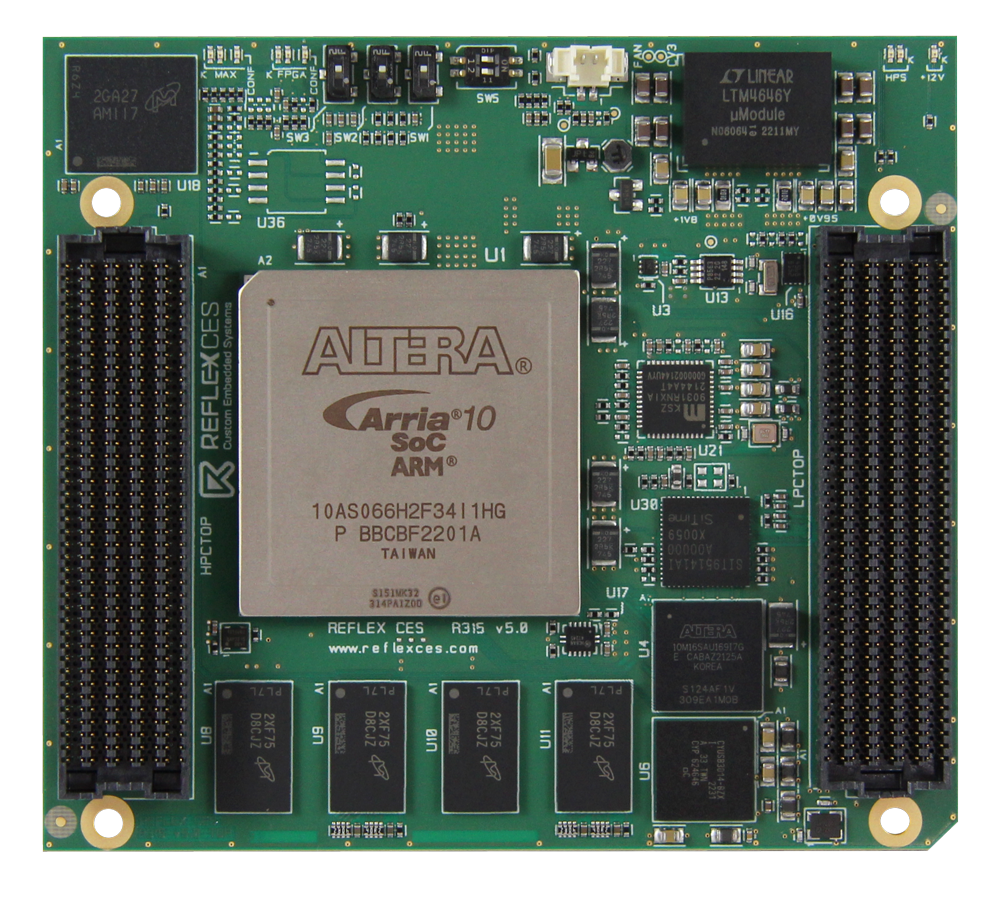
The size of the SoM is 86mm x 95 mm
The figures into the Carrier design Guide documentation shows the Arria® 10 SoC SoM form factor with connector and attachement holes position, views from the TOP side of the board, dimensions in millimeters. Detailled STEP File of the Arria® 10 SoC SoM is available upon request, please contact support or your sale representative for more information.
Le module Achilles Arria® 10 SoC est basé sur le FPGA Intel® Arria® 10 SoC, et est disponible en 3 versions différentes, en fonction du FPGA, de la mémoire et des connecteurs voulus (voir l’onglet “Tech Spec”).
Avec son ARM double-coeur Cortex-A9 MPCore et jusqu’à 660 KLEs dans le FPGA d’éléments logiques à faible consommation, le PFGA Arria® 10 SoC combine la flexibilité et la facilité de programmation d’un CPU avec la configurabilité et la puissance de traitement parallèle d’un FPGA.
Sa petite taille et son FPGA puissant le rendent parfaitement adapté aux marchés de l’embarqué et de l’industrie.
Grâce à son SoC (system-on-chip) (un circuit intégré à l’intérieur du FPGA, le plus souvent un processeur CPU – central processing unit), le FPGA peut mieux contrôler la carte.
Les marchés cibles incluent l’industrie automobile, la diffusion vidéo, la vision intelligente par ordinateur, l’industrie, le militaire, les tests & mesures, et le medical.
Le module Achilles Arria® 10 SoC est expédié seul.
➡️ Il peut aussi être disponible dans un Kit de Développement: le Kit Achilles. Ce kit de développement pour module Arria® 10 SoC vous fournira en plus des schémas, les reference design, ainsi qu’une starter board.
➡️ Nous vous proposons aussi en option la carte porteuse PCIe, compatible avec tous nos modules Arria® 10 SoC de reflex ces. Nous pouvons sinon vous concevoir une carte porteuse sur-mesure.
La carte porteuse PCIe Achilles Arria® 10 SoC donne accès à l’ensemble des fonctionnalités du module Achilles Arria® 10 SoC (ethernet, OTG USB, Transceivers, UART) et inclus aussi des fonctions supplémentaires telles que des connecteurs SFP+, PCIe x8 Gen3, USB3.0, et une interface Wifi.
Cette carte porteuse PCIe est un produit en option pour les clients qui recherchent une carte au format PCIe.
Tous les produits de type modules à base de SoC Intel® Arria® 10 (Module Achilles, DevKit Achilles) peuvent être utilisés conjointement avec la carte porteuse PCIe. Nous pouvons aussi vous concevoir une carte porteuse sur-mesure.
Les marchés cibles incluent l’industrie automobile, la diffusion vidéo, la vision intelligente par ordinateur, l’industrie, le militaire, les tests & mesures, et le medical.