


Presentation of the Virtex™ Ultrascale+™ VU5P or VU9P FPGA PCIe board
The XpressVUP-LP5/9PT2 Virtex™ Ultrascale+™ VU5P / VU9P FPGA PCIe board is a low-profile PCIe network processing FPGA board.
The XpressVUP-LP5/9PT2 Virtex™ Ultrascale+™ VU5P / VU9P FPGA PCIe board is either based on a AMD Virtex™ Ultrascale+™ VU5P FPGA, or on a AMD Virtex™ Ultrascale+™ VU9P FPGA. The device provides the highest performance and integration capabilities in a 14 nm/16 nm FinFET node, the VU9P offering more System Logic Cells.
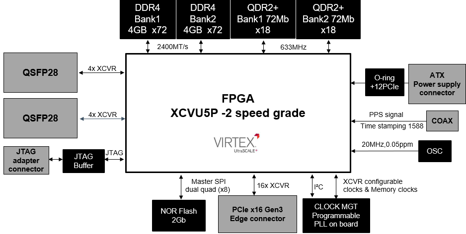
The board provides 2 banks of DDR4, 2 banks of QDR2+ memories, and two QSFP28 cages for multi 10 GbE/40 GbE/100 GbE networking solutions.
The FPGA board is delivered with a PCIe standard or low-profile bracket, and was specifically designed to optimize embedded applications.
This low-profile PCIe board is designed for computationally intensive applications, from HPC to networking.
If you are looking for more performances, check the XpressVUP-LP9PT3 Virtex™ Ultrascale+™ VU9P-3 FPGA PCIe board.
If you are looking for an industrial type of board, with conduction cooled heat system, check the XpressVUP-LP9PTI Virtex™ Ultrascale+™ VU9P-2 FPGA PCIe board.
Benefits
The XpressVUP-LP5/9PT2 Virtex™ Ultrascale+™ VU5P / VU9P FPGA PCIe board is a low-profile FPGA board, compliant with RoHS/REACH, ISO 9001 and UL standards.
The board is based on the AMD Virtex™ Ultrascale+™ VU5P or VU9P semiconductor FPGA. The device is ideal for computationally intensive applications.
FPGAs (field programmable gate arrays) are used to offer high-capacity logic and memory storage.
Our Virtex™ Ultrascale+™ VU5P/VU9P FPGA PCIe board offers primary interfaces and components, such as PCB and circuitry, 100 GB ethernet, PCI-Express slot, DDR4 and QDR2+ memories, JTAG connector, transceivers, clock, power supply, power connector, and more (see Specifications tab).
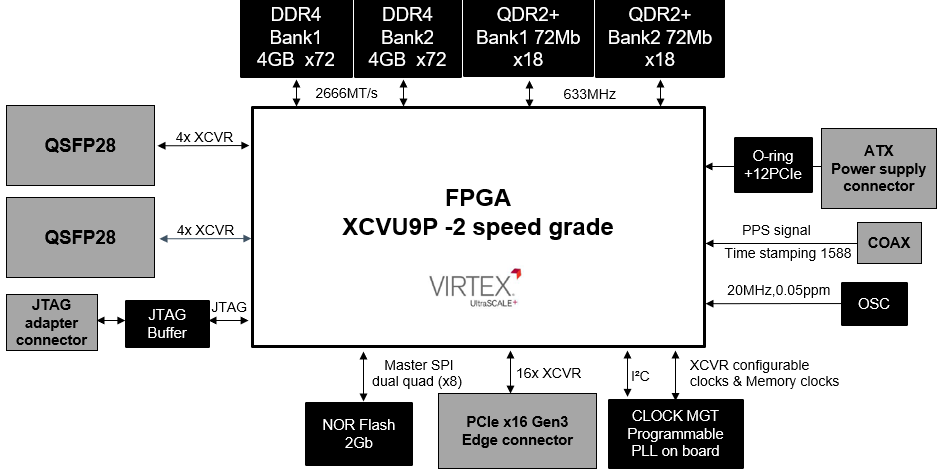
The Peripheral Component Interconnect Express, commonly known as PCI Express, is a high-speed serial computer expansion bus standard. Our FPGA board offers a PCI-Express x16 slot. Added to an AMD Virtex™ Ultrascale+™ VU9P FPGA, it makes our board quick and efficient.
The form factor of the Virtex™ Ultrascale+™ VU5P/VU9P FPGA PCIe board is low-profile.
We draw on our firmware HDL, hardware and embedded software skills, available schematics, datasheet, and design tools, to program the FPGA board to fit into embedded systems.
With its perfectly suited Virtex™ Ultrascale+™ VU9P FPGA design, this evaluation board offers rapid prototyping for a quick time to market.
The board is delivered with a custom passive heatsink, and can be integrated into a chassis.
Our Virtex™ Ultrascale+™ VU5P/VU9P FPGA development board is specially designed for customer needs and specifications.
Our sales team is available to advise you on the best solution according to your needs, at sales@reflexces.com.
Block diagram of the Virtex™ Ultrascale+™ VU5P FPGA PCIe board:
Block diagram of the Virtex™ Ultrascale+™ VU9P FPGA PCIe board:
FPGA and configuration modules
OR
Communication Interfaces
Memory
Operating Range & Power
Other resources
Board Dimensions
Standards and compliance
Board content
Ordering information
XpressVUP-LP5PT2: VU5P speed grade -2L, XCVU5P-L2FLVB2104E
XpressVUP-LP9PT2 : VU9P speed grade -2; XCVU9P-2FLGB2104E
ECCN Number : 4A994i
CECC (commodity Export Classification Certificate) : Download XpressVUP-LP9PT2 certificate
CECC (commodity Export Classification Certificate) : Download XpressVUP-LP5PT2 certificate

The XpressVUP-LP5PT2 is based on a Virtex® Ultrascale+™ VU5P FPGA. This Virtex® Ultrascale+™ VU5PT2 FPGA PCIe board is a low-profile PCIe network processing FPGA board.
The Virtex® Ultrascale+™ VU5P FPGA provides the highest performance and integration capabilities in a 14 nm/16 nm FinFET node. As the industry’s most capable FPGA family, this device is ideal for computationally intensive applications.
The board provides 2 banks of DDR4, 2 banks of QDR2+ memories, and two QSFP28 cages for multi 10 GbE/40 GbE/100 GbE networking solutions.
The FPGA board is delivered with a PCIe standard or low-profile bracket. The Virtex® Ultrascale+™ VU5P FPGA PCIe board was specifically designed to optimize embedded applications.
This low-profile PCIe board is designed for acceleration, data centers, networking, and security applications.
If additional System Logic Cells are required, check the XpressVUP-LP9P Virtex® Ultrascale+™ VU9P FPGA PCIe board.
If you are looking for more performances, check the XpressVUP-LP9PT3 Virtex® Ultrascale+™ VU9P-3 FPGA PCIe board.
The XpressVUP-LP9PT3 Virtex™ Ultrascale+™ VU9P-3 FPGA PCIe board is a low-profile PCIe network processing FPGA board, optimized for HFT (high frequency trading) and Ultra low-latency.
The XpressVUP-LP9PT3 Virtex™ Ultrascale+™ VU9P-3 FPGA PCIe board is based on an AMD Virtex™ Ultrascale+™ VU9P-3 FPGA, with -3 speed grade.
The board provides 2 banks of DDR4, 2 banks of QDR2+ memories (2 chips of 288 Mbit for a 576 Mbit total of external QDR2+), and two QSFP28 cages for multi 10 GbE/40 GbE/100 GbE networking solutions.
The FPGA board is delivered with a dual slot active heatsink, and was specifically designed to optimize embedded applications.
This low-profile PCIe board is designed for computationally intensive applications, from HPC to finance and networking.
Advantages of using our Virtex™ Ultrascale+™ VU9P-3 FPGA board in finance applications include high performance, low latency, and enhanced security. Fintech is a domain in which companies increasingly require the most innovative and high-end FPGA technologies for their key applications listed on the stock exchanges and the banks. Such FPGA boards enable financial institutions to accelerate computations, make faster trading decisions, and optimize their financial strategies, ultimately gaining a competitive edge in the dynamic world of finance.
For a different speed grade, check the XpressVUP-LP5/9PT2 Virtex™ Ultrascale+™ VU9P FPGA PCIe board.