


Presentation of the Arria ® 10 SoC som
The Arria® 10 SoC SOM is based on the Intel® Arria® 10 SoC FPGA, and is available in three different versions according to the FPGA, memory, and connectors needed (see the “Tech Spec” tab).
Featuring an ARM dual-core Cortex-A9 MPCore and up to 660 KLEs of advanced low-power FPGA logic elements, the Arria® 10 SoC combines the flexibility and ease of programming of a CPU with the configurability and parallel processing power of an FPGA.
Its small size and its strong FPGA makes it perfectly suited to embedded and industrial markets.
Thanks to a system-on-chip (SoC) (an integrated circuit inside the FPGA, most often a CPU (central processing unit) processor), the FPGA can better control the board.
The target markets include automotives, video broadcasting, machine and intelligent vision, industry, military, testing and measurements, and medical.
The Arria® 10 SoC SOM is shipped alone.
➡️This System On Module is also available in a Development Kit : The Achilles DevKit. This Arria ® 10 SoC development kit will provide you with schematics, reference designs and a starter board.
➡️We also offer a PCIe Carrier Board as an optional extra product compatible with all reflex ces Arria® 10 SoC SOMs, or we can design a custom carrier board.
The Intel® Arria® 10 SoC family integrates a Dual-Core ARM Cortex-A9 MPCore, hardened floating-point variable-precision digital signal processing (DSP) blocks, along with high-speed transceivers and on-chip memory.
REFLEX CES’s Arria® 10 SoC SOM offers a range of interfaces according to your needs
Our Arria® 10 SoC SOM offers primary interfaces, such as several banks of DDR4 memory, I2C and USB links, FMC connectors (with many available LVDS/single ended I/Os), JTAG connectivity, CPU, peripherals, switches, ethernet interfaces. We also deliver all the relevant design rules for our boards, to develop the customer application carrier board (we can also develop it based on customer specifications). We provide online technical support and schematics, and several certifications may be available on request.
The Arria 10 SoC FPGA is a semiconductor that saves board space with integration, with twice the density of the previous generation. This leads to lower energy requirements and therefore lower power consumption. Our system-on-module is designed for productivity and is perfectly suited to embedded and industrial markets.
Our Arria ® 10 SoC som is specially designed for customer needs. Our sales team is available to advise you on the best solution according to your needs, at sales@reflexces.com.
Find out more on rocketboards:
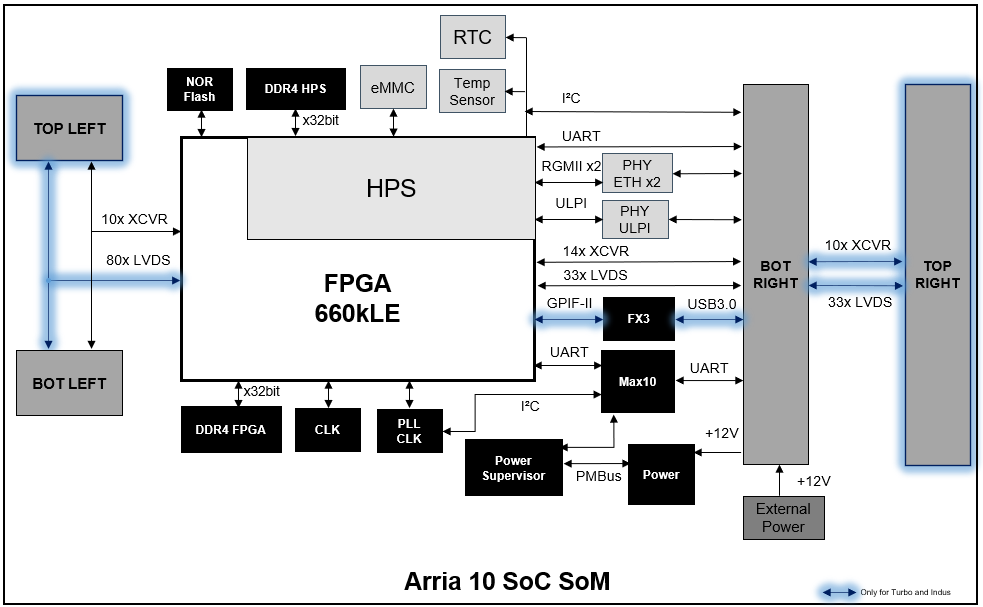
Block diagram of the Arria ® 10 SoC som:
Full specifications
| Features | Description | Achilles "Lite" 12G V5 | Achilles "Indus" V5 | Achilles "Indus" 12G V5 |
| FPGA SoC | Arria® 10 SoC, F34 package (1152 pins) | 10AS027H3F34E2SG, speed grade -2 270KLE, 830 DSP Blocks Dual-Core ARM® Cortex®-A9 MPCore Processor | 10AS066H2F34I1HG, speed grade -1 660KLE, 1688 DSP Blocks Dual-Core ARM® Cortex®-A9 MPCore Processor | |
| DDR4 Memory | 32bit wide bank for FPGA | 4GByte @2133MT/s | 4GByte @2400MT/s | |
| 32bit wide bank for HPS | 3GByte @2133MT/s | 3GByte @2400MT/s | ||
| Communication & Networking | 2x Gigabit Ethernet RGMII on the HPS USB 2.0 host/device OTG support connected to the HPS I²C link support connected to the HPS,EEPROM, Sensor Temp UART connected to System controller and to HPS | |||
| No USB 3.0 X | USB 3.0 using Cypress FX3 super speed controller | |||
| FMC Connectors | Top Left High Pint Count (HPC) | X | Power Suplies Output: +12/+3.3V/1.8V/ +VADJ = +1.8V 80 LVDS pairs (1.25Gbps) or 160 single ended LVCMOS1.8V 10 Serial transceiver channels (RX and TX) @7Gbps | X |
| Top Right Low Pin Count (LPC) | X | Power Suplies Output: +12/+3.3V/1.8V/ +VADJ = +1.8V 33 LVDS pairs (1.25Gbps) or 68 single ended LVCMOS1.8V 10 Serial transceiver channels (RX and TX) @7Gbps | X | |
| Bottom Left High Pint Count (HPC) | No Power supply, respect +VADJ electrical standard (+1.8V) | |||
| 34 LVDS pairs (1.25Gbps) or 68 single ended LVCMOS 1.8V | 80 LVDS pairs (1.25Gbps) or 160 single ended LVCMOS 1.8V | |||
| 10 Serial transceiver channels (RX and TX) @12Gbps | 10 Serial transceiver channels (RX and TX) @7Gbps | 10 Serial transceiver channels (RX and TX) @12Gbps | ||
| Bottom Right Low Pin Count (LPC) | Power Suply +12V Hard Processing ARM peripheral I/Os (GbE,USB2.0,I²C,UART) | |||
| 33 LVDS pairs (1.25Gbps) or 68 single ended LVCMOS 1.8V FPGA peripheral I/Os (GPIF II= USB3.0) | ||||
| 14 Serial transceiver channels (RX and TX) @12Gbps | 4 Serial transceiver channels (RX and TX) @10Gbps 10 Serial transceiver channels (RX and TX) @7Gbps | 14 Serial transceiver channels (RX and TX) @12Gbps | ||
| FPGA Configuration | Onboard JTAG configuration circuitry to enable configuration over USB | Onboard JTAG configuration circuitry to enable configuration over USB | ||
| 512Mb Quad SPI Flash for remote upgrade and failsafe configuration | 512Mb Quad SPI Flash for remote upgrade and failsafe configuration | |||
| Software Configuration | Nand Flash eMMC (Store operating Linux system : U boot, Kernel and RootFS) | 32GByte | ||
| Module dimensions | 83.1 x 95 mm (3.3 x 3.8 inches) | |||
| Weight | Lite 12G module without Mechanics: 78.8g Heat Spreader: 93.9g | Heat Sink: 86.9g | Fan: 15.7g | Indus/Indus 12G module without Mechanics: 87.8g Heat Spreader: 93.9g | Heat Sink: 86.9g | Fan: 15.7g | ||
| Temperature range | Commercial | Industrial | ||
| Deliverables | Arria® 10 SoC module (+ heat spreader, heat sink and fan) | |||
| Ordering Information | RXCA10S027PF34-SOM12L | RXCA10S066PF34-SOM02I | RXCA10S066PF34-SOM12I | |
Arria® 10 SoC disruptive System-on-Module by REFLEX CES :
Achilles Workshop by REFLEX CES :
Object detection demo using FPGA DNN IP :
Below are the videos regarding The Achilles DevKit :
Setting up your REFLEX CES Achilles Development Kit :
Exploration of REFLEX CES' Graphical User Interface (GUI) for the Achilles Development Kit :
Deliverables
The following deliverables are only included with the purchase of an Arria® 10 SoC SoM Instant-DevKit:
ECCN Number : 4A994i
CECC (commodity Export Classification Certificate) : Download certificate
FPGA resources (HPS included)
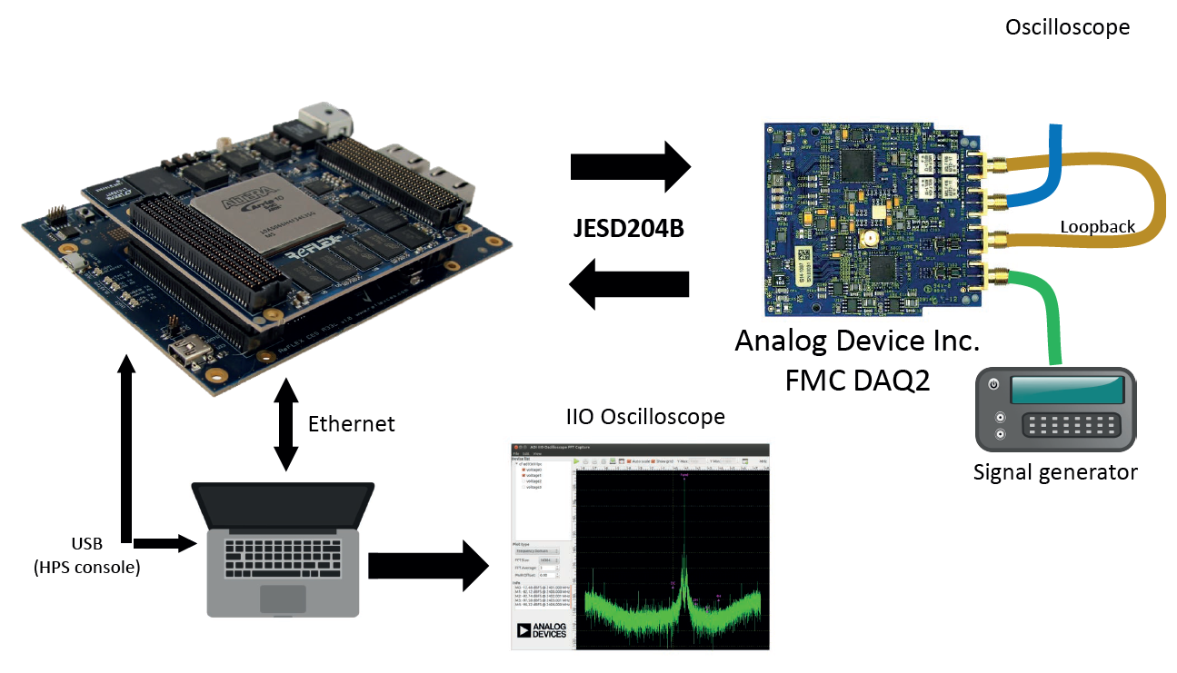
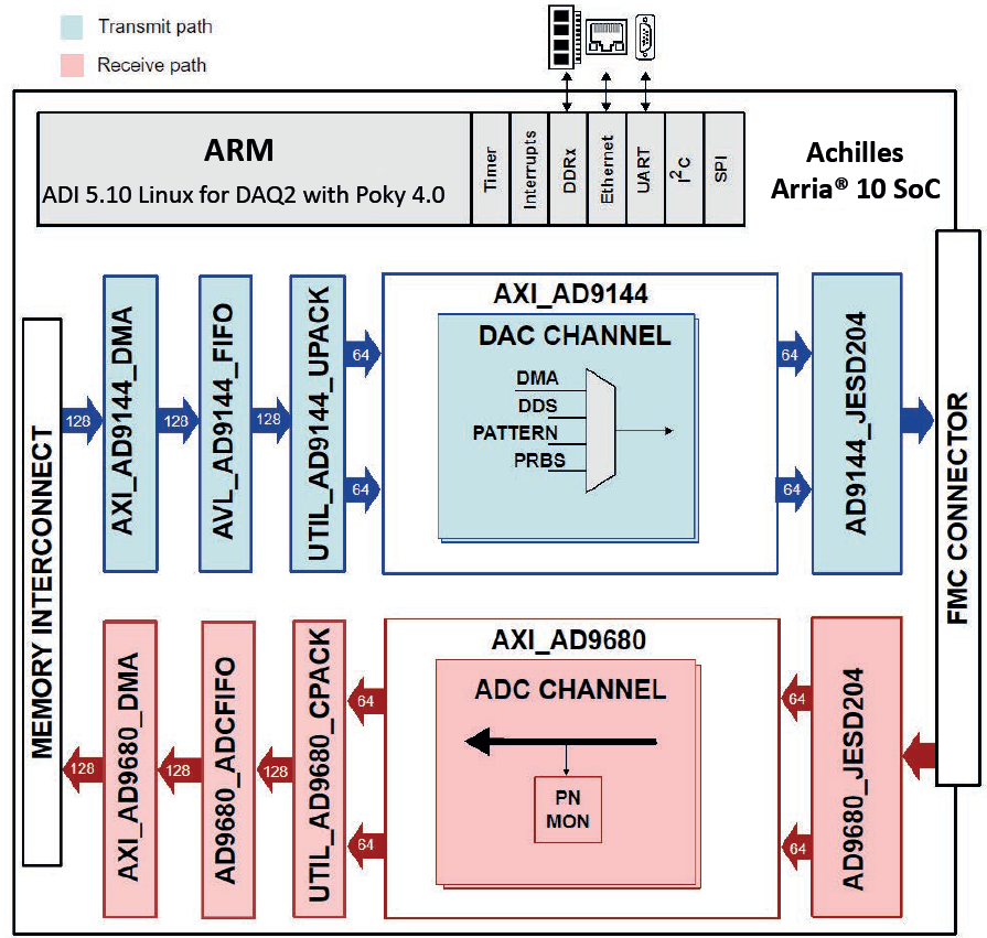
ADC, DAC and JESD204B setup
Power*
* Including FAN: 1.3W
** Quartus Power Estimator
The Arria® 10 SoC development kit is based on the Intel® Arria® 10 SoC FPGA. It includes an Arria® 10 SoC system-on-module, a starter board, and all the schematics and reference designs needed to start working on the board.
Featuring an ARM dual-core Cortex-A9 MPCore and up to 660 KLEs of advanced low-power FPGA logic elements, the Arria® 10 SoC combines the flexibility and ease of programming of a CPU with the configurability and parallel processing power of an FPGA.
Thanks to a system-on-chip (SoC) (an integrated circuit inside the FPGA, most often a CPU (central processing unit) processor), the FPGA can better control the board.
Its small size and its strong FPGA makes it perfectly suited to embedded and industrial markets.
The target markets include automotives, video broadcasting, machine and intelligent vision, industry, military, testing and measurements, and medical.
REFLEX CES also markets the A10 SoC SoM separately. We also offer a PCIe Carrier Board as an optional extra, or we can design a custom carrier board.

The Arria® 10 SoC SOM carrier board provides access to all the features of the Achilles Arria® 10 SoC system-on-module (ethernet, OTG USB, Transceivers, UART) and includes further functions, such as SFP+ connectors, PCIe x8 Gen3, USB3.0, and a Wifi interface.
This PCIe Carrier Board is an optional extra product for clients looking for a PCIe format card.
All REFLEX CES Achilles Arria® 10 SoC SoM products (Achilles Arria® 10 SoC system-on-module, Achilles Arria® 10 SoC SoM Development Kit) can be used in conjunction with the PCIe Carrier Board. We also can design a custom carrier board.
The target markets include automotives, video broadcasting, machine and intelligent vision, industry, military, testing and measurements, and medical.