


Presentation of the Ares Agilex™ 7 FPGA SoC F-Series module
The Ares SoM is an Agilex™ SoC F-Series system-on-module, based on the Intel® Agilex™ 7 FPGA SoC F-Series FPGA. The main advantage of the Agilex™ 7 SoC F-Series FPGA is its flexibility and high-performance capabilities, enabling designers to efficiently implement complex algorithms and integrate multiple functions onto a single chip, resulting in reduced power consumption, and improved system performance and technology.
The system-on-module (module SoM) is delivered with an active heatsink with heat spreader and fan, and is specifically optimized for embedded applications. Using a module for an embedded system can simplify the design process and reduce time-to-market by providing pre-built, tested components that can be easily integrated into your system.
Target markets of this Agilex™ SoC F-Series module include Bioscience & Instrumentation, Quantum Computing, Radar Systems, Electronic Warfare, Satellite Communication, and much more.
➡️ We also offer the Ares carrier board for the Ares Agilex™ SoC F-Series module, fully developed and compatible with its module.
This module offers an Intel® Agilex™ 7 SoC F-Series FPGA technology.
Intel® Agilex™ F-Series devices are general-purpose FPGAs built on Intel 10 nm SuperFin process technology. The Intel® Agilex™ 7 SoC F-Series FPGA is part of the Agilex™ SoC family.
FPGAs (field programmable gate arrays) like Agilex™ SoC F-Series module and Agilex™ FPGA are used to offer high-capacity logic and memory storage.
Programmable logic and accelerator technologies such as Agilex™ FPGA chips can improve system performance while reducing power consumption. These accelerators can be programmed using embedded programming languages and integrated into the system design using industry-standard interfaces.
FPGA chips, including Agilex™ FPGA device, can be programmed using embedded programming languages such as VHDL or Verilog, and can be integrated into the system design using industry-standard interfaces such as PCI Express (PCIe = Peripheral Component Interconnect Express). They can be used to perform tasks such as image processing, data compression, and encryption more quickly and with less power consumption than a traditional processor.
The system-on-chip (SoC) is an integrated circuit inside the FPGA, most often a CPU (central processing unit) processor and supporting peripherals, that provides more flexibility and integration, and allows the FPGA to better control the board.
reflex ces included numerous essential components for an embedded board, developed for this intel agilex FPGA: PCB (Printed Circuit Board), transceivers, power supply, JTAG, DDR4, Flash eMMC memory, BMC (Baseboard Management Controller), and more.
Embedded programming is an essential part of developing embedded systems. Our designers carefully consider the architecture of the FPGA chip and the system design to ensure that the accelerator is correctly integrated into the system. They also consider the programming and debugging tools available for the FPGA chip, such as Intel Agilex™, to ensure efficient development and testing.
Reduce time to market of your next embedded project with our Agilex™ 7 FPGA SoC module, Agilex™ FPGA SoC board, using the Intel® Quartus Prime development tools. We draw on our firmware, hardware and software skills, and full documentation package and reference designs to create our boards.
The Intel® Agilex™ 7 FPGA SoC board is RoHS (Restriction of Hazardous Substances) and REACH (Registration, Evaluation, Authorization, and Restriction of Chemicals) standard compliant.
Our designers always keep the industry standard and footprint in mind when developing embedded systems. Standard interfaces and architectures, ensure that the card and the system can be efficiently integrated into the larger ecosystem. The footprint of the system is also carefully considered, ensuring that it fits within the size constraints of the final product. With these considerations in mind, they create efficient and effective embedded systems that are ready to market.
Our Ares Agilex™ 7 FPGA SoC F-Series system-on-module, Intel Agilex™ FPGA device, and Agilex™ SoC is specially designed for customer needs. Our sales team is available to advise you on the best solution according to your needs and product specifications, at sales@reflexces.com
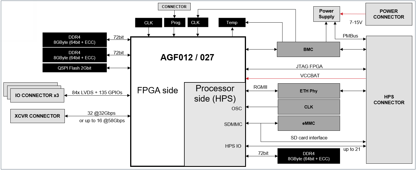
Block diagram of the Ares Agilex™ 7 FPGA SoC F-Series module:
Module dimension: 107mm x 85mm (4.2 x 3.4 inches)
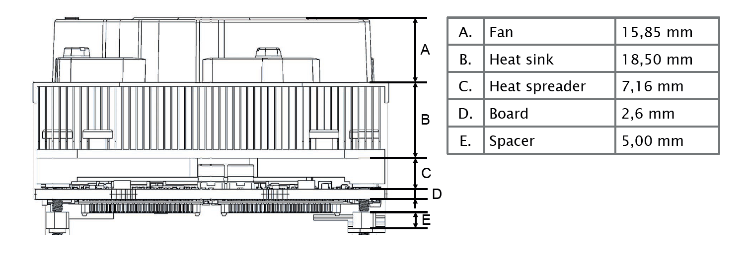
Module + heatspreader: 14.76mm
Module + heatspreader + passive heat sink: 33.26mm
Module + heatspreader + passive heat sink + fan: 49.11mm
| Features | Ares Agilex™ 7 FPGA SoC F-Series | |
| Ordering Information | RXCAGF012PR24-SOM00I (in production)using AGFB012R24C2I2V (1.2MLE) 1178 KLE, 110Mbit M20K, 3743 DSP Blocks | RXCAGF027PR24-SOM00I (in production)using AGFB027R24C2I1VC (2.7MLE) 2693 KLE, 259Mbit M20K, 8528 DSP Blocks |
| FPGA SoC | Agilex™ 7 FPGA SoC F-Series R24C package, pin compatible from 600KLE (AGF006) up to 2.7MLE (AGF027) Quad Core Arm Cortex-A53 up to 1.43GHz Industrial Temp Grade | |
| Transceiver speed grade 2, Core speed grade 2 | Transceiver speed grade 2, Core speed grade 1 | |
| DDR4 Memory | 3 banks DDR4, 24 GByte total | |
| HPS= 1 bank DDR4 x72bit bus, 8GByte, @2666MT/s FPGA= 2 banks DDR4 x72bit bus, 8GByte each, @2666MT/s | HPS= 1 bank DDR4 x72bit bus, 8GByte, @3200MT/s FPGA= 2 banks DDR4 x72bit bus, 8GByte each, @3200MT/s | |
| Connectors | Transceiver Mezzanine Connector: 32 transceivers @32Gbps NRZ OR up to 16 transceivers @58Gbps PAM4 (example: 16 transceivers @32Gbps NRZ + 8 @58Gbps PAM4) | |
| IO Mezzanine Connector: FPGA GPIOs = 135 HPS IO = up to 21 depending used interfaces | ||
| LVDS = 38 RX pairs and 38 TX pairs @1400Mbps | LVDS = 38 RX pairs and 38 TX pairs @1600Mbps | |
| FPGA Configuration | 2Gbit Quad SPI Flash (store up to 2 images) | |
| Software Configuration | 128Gbyte NAND Flash eMMC (Stores U-Boot, Linux Kernel, and RootFS) + SD Card support on the carrier board (RXCAGF-CBD0SA) | |
| HPS Communication | 1GbE RGMII, I2C, UART, USB 2.0 OTG, SPI slave and master, HPS IO | |
| Mechanical & Environmental Specification (to be qualified) | Module rugged for shocks and high vibration IEC/EN61000 (EMI immunity), EN61000 + EN55032 (EMI emission), EN60068 (Vibration: sinusoidal, 10Hz - 2KHz, +/- 0.15mm, 2g ; Shock: half-sinusoidal, 11ms, 15g) 7-15V Power Input Industrial temperature grade -40°C to +70°C | |
| Power & dissipation | Typ 113W, active airflow cooling (heat spreader + heatsink + fan) | Max 122.5W | Typ 161W, active airflow cooling (heat spreader + heatsink + fan) | Max 171W |
| fan noise < 50dB, fan control capability (PWM, TACHY) | ||
| Board Management Controller | Communication with Carrier board: I2C, JTAG Communication with FPGA : 1x UART to FPGA Monitoring : Current, voltages, temperature, ID information Programming : Clock Control: Power, temperature protection, Fan | |
| Module dimensions and weight | 107mm x 85mm (4.2 x 3.4 inches) weight without mechanics: 125g | |
| Compliance | RoHS/REACH compliant | |
| Deliverables | • Ares module & its active cooling system • Board Support Package (to download from our online technical support) after purchase of a module and its carrier board: Starter Guide, module and carrier board Reference Manuals, Interconnect pinout file Mechanical drawings, assembly files FPGA GSRD Test Design by interface (Quartus Prime Pro Edition 24.2) BMC Software API HPS Software: -- Built with Yocto Project version 4.2 (Mickledore) -- U-Boot bootloader (v2023.04), ATF Linux kernel (v6.1.38) and linux Poky distribution • 1-year technical support and warranty • Online support at support.reflexces.com (after purchase of a kit) | |
| MOTS = Modified version (on request) | • Conformal coating • Custom heatsink system • Contact sales for customization | |
Altera™ Agilex™ 7 is a high-performance FPGA and SoC FPGA family designed for next-generation embedded systems requiring high computing performance, advanced connectivity, and low-latency data processing.
Based on altera™’s advanced FPGA architecture, Agilex™ 7 devices combine a programmable FPGA fabric with high-speed transceivers and, in SoC variants, an integrated ARM processor subsystem. This heterogeneous architecture enables designers to combine real-time processing, hardware acceleration, and embedded computing within a single device.
The Agilex™ 7 SoC F-Series integrates a quad-core ARM Cortex-A53 processor with FPGA programmable logic, allowing developers to run embedded software applications while implementing performance-critical functions directly in hardware.
Key features of altera™ Agilex 7 FPGA SoC devices include:
Compared with previous FPGA families such as Arria® 10 or Stratix® 10, Agilex™ 7 delivers significant improvements in processing capability, connectivity, and flexibility, making it suitable for demanding applications requiring real-time processing and deterministic performance.
By integrating Agilex™ 7 FPGA technology into a System-on-Module (SoM) architecture, companies can accelerate embedded system development while reducing design complexity and time-to-market.
Agilex™ 7 SoC F-Series is designed to combine FPGA fabric and an integrated ARM Cortex-A53 processing subsystem in a single device, enabling a tightly coupled hardware and software architecture for embedded systems.
It allows real-time hardware acceleration of compute-intensive tasks while maintaining full software flexibility on the embedded processor. This heterogeneous approach enables deterministic low-latency performance for applications that cannot be handled efficiently by CPUs alone.
The architecture supports parallel processing through FPGA logic while the processor handles control, operating system execution, and high-level functions. It also integrates high-speed transceivers and PCIe interfaces to support modern data-intensive embedded designs.
By combining processing, acceleration, and connectivity in one SoC FPGA, this architecture reduces system complexity and board footprint compared to discrete CPU and FPGA implementations. It also improves development efficiency by simplifying hardware integration and software-hardware partitioning, while maintaining optimized power consumption for high-performance embedded platforms.
Agilex™ 7 FPGA SoC technology is used in embedded systems that require high-performance computing, real-time processing, and deterministic low-latency execution across demanding industries.
Radar systems rely on Agilex™ 7 FPGA SoCs to process large volumes of high-frequency sensor data in real time. The FPGA fabric enables fast signal processing chains, filtering, and beamforming operations, while maintaining strict timing constraints required in modern radar architectures.
Electronic Warfare and defense systems use Agilex™ 7 SoC devices for signal intelligence, spectrum analysis, and adaptive signal processing. The combination of FPGA acceleration and embedded ARM processing allows both high-speed computation and system-level control within the same architecture.
Software Defined Radio applications benefit from the flexibility of Agilex™ 7 FPGA SoCs to implement multiple communication standards and dynamically reconfigurable waveforms. This enables the same hardware platform to support evolving protocols and mission requirements.
High-speed data acquisition systems use Agilex™ 7 FPGA modules to capture, process, and analyze large data streams from sensors and instrumentation equipment. The parallel processing capabilities of the FPGA enable real-time handling of multi-channel, high-bandwidth data.
Aerospace and defense embedded computing platforms use Agilex 7 SoC FPGAs for mission-critical processing tasks that require long lifecycle support, reliability, and high computational performance in constrained environments.
Edge AI applications leverage Agilex 7 FPGA SoCs to perform inference directly at the edge, reducing latency and bandwidth usage while enabling real-time decision-making close to the data source.
Deliverables for the purchase of a System-on-Module:
Ordering information:
RXCAGF012PR24-SOM00I using AGFB012R24C2I2V FPGA
RXCAGF027PR24-SOM00I using AGFB027R24C2I1VC FPGA
Availability: in production
ECCN Number : 5A002
CECC (commodity Export Classification Certificate) : Download certificate
The Ares Agilex™ 7 SoC F-Series system-on-module 6U VPX carrier board is an evaluation board with a FMC+ connector.
This evaluation Agilex™ 7 SoC F-Series board was designed to complement the reflex ces Module.
The target applications of our Agilex™ 7 SoC F-Series carrier board include bioscience & instrumentation, quantum computing, radar systems, satellite communication and electronic warfare.
The Ares carrier board is fully compatible with the Ares Module.

The Arria® 10 SoC SOM is based on the Intel® Arria® 10 SoC FPGA, and is available in three different versions according to the FPGA, memory, and connectors needed (see the “Tech Spec” tab).
Featuring an ARM dual-core Cortex-A9 MPCore and up to 660 KLEs of advanced low-power FPGA logic elements, the Arria® 10 SoC combines the flexibility and ease of programming of a CPU with the configurability and parallel processing power of an FPGA.
Its small size and its strong FPGA makes it perfectly suited to embedded and industrial markets.
Thanks to a system-on-chip (SoC) (an integrated circuit inside the FPGA, most often a CPU (central processing unit) processor), the FPGA can better control the board.
The target markets include automotives, video broadcasting, machine and intelligent vision, industry, military, testing and measurements, and medical.
The Arria® 10 SoC SOM is shipped alone.
➡️This System On Module is also available in a Development Kit : The Achilles DevKit. This Arria ® 10 SoC development kit will provide you with schematics, reference designs and a starter board.
➡️We also offer a PCIe Carrier Board as an optional extra product compatible with all reflex ces Arria® 10 SoC SOMs, or we can design a custom carrier board.